World's smallest all-digital circuit created, scientists say

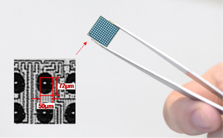
Scientists at the Tokyo Institute of Technology (Tokyo Tech) and system-on-chip company Socionext have designed what they claim is the world’s smallest all-digital phase-locked loop (PLL) — a critical clocking circuit that is used in virtually all digital applications — fitting in an area measuring just 50 x 72 µm2.
Technologies such as artificial intelligence, 5G and the IoT are expected to bring revolutionary changes to society — but for that to happen, high-performance system-on-chip (SoC) devices are indispensable. A core building block of SoC devices is the PLL — a circuit that synchronises with the frequency of a reference oscillation and outputs a signal with the same or higher frequency. PLLs generate ‘clocking signals’, whose oscillations act as a metronome that provides a precise timing reference for the harmonious operation of digital devices.
For high-performance SoC devices to be realised, fabrication processes for semiconductor electronics must become more sophisticated. The smaller the area to implement digital circuitry is, the better the performance of the device. 7 nm semiconductors (a big improvement over their 10 nm predecessor) are already in production, and methods to build 5 nm devices are now being examined. However, existing PLLs require analog components, which are generally bulky and have designs that are difficult to scale down.
The Tokyo Tech scientists addressed this issue by implementing a ‘synthesisable’ fractional-N PLL, which requires only digital logic gates and no bulky analog components, making it easy to adopt in conventional miniaturised integrated circuits. Their work has been described in the journal IEEE Solid-State Circuits Letters.
Led by Professor Kenichi Okada, the team used several techniques to decrease the required area, power consumption and jitter (unwanted time fluctuations when transmitting digital signals) of their synthesisable PLLs. To decrease area, they employed a ring oscillator — a compact oscillator that can be easily scaled down. To suppress jitter, they reduced the phase noise (signal fluctuations) of this ring oscillator by using ‘injection locking’ — the process of synchronising an oscillator with an external signal whose frequency (or multiple of it) is close to that of the oscillator — over a wide range of frequencies. The lower phase noise, in turn, reduced power consumption.
The team claims their synthesisable PLL surpasses current state-of-the-art PLLs in many aspects, achieving the best jitter performance with the lowest power consumption and smallest area: “The core area is 0.0036 mm2, and the whole PLL is implemented as one layout with a single power supply,” Prof Okada noted. Furthermore, it can be built using standard digital design tools, allowing for rapid, low-effort and low-cost production and thus making it commercially viable.
The synthesisable PLL can also be easily integrated into the design of all-digital SoCs, making it valuable for developing a 5 nm semiconductor for applications including artificial intelligence and IoT, where high performance and low power consumption are critical. The research also demonstrates the potential of synthesisable circuits, with Prof Okada noting, “With the design methodology employed here, other building blocks of SoCs, such as data converters, power management circuits and wireless transceivers, could be made synthesisable as well. This would greatly boost design productivity and considerably reduce design efforts.”
Tokyo Tech and Socionext will continue their collaboration in this field to advance the miniaturisation of electronic devices, enabling the realisation of next-generation technologies.
Please follow us and share on Twitter and Facebook. You can also subscribe for FREE to our weekly newsletter and bimonthly magazine.
3D semiconductor chip alignment boosts performance
Researchers have developed an ultra-precise method to align 3D semiconductor chips using lasers...
Researchers achieve 8 W output from optical parametric oscillator
Researchers have demonstrated a total output power of 8 W from a high-power mid-infrared cadmium...
"Dualtronic" chip for integrated electronics and photonics
Cornell researchers have developed a dual-sided chip known as a "dualtronic" chip that...


