
Probing for accurate baseband I/Q measurements
Wednesday, 02 December, 2009
In modern digital communications systems the information content is typically created digitally and then used to modulate an RF signal. It is useful to evaluate the modulation, both before and after upconversion to diagnose any impairments in the conversion process.
In some cases a single complex, mixed-mode integrated circuit (ASIC) is used to convert from the digital domain directly to RF.
This is shown in Figure 1a. In this case, a logic analyser can be used to evaluate the input digital pattern and interpret it as digital I/Q modulation data using signal analysis software.
|
|
 Figure 1a: Directly upconverting digital modulation onto an RF carrier with a monolithic mixed-signal ASIC.
A vector signal analyser can be used to evaluate the RF signal, including the modulated information content. The same signal analysis software can be employed in both the RF and digital domains.
In many cases the upconversion process is split into two steps, as shown in Figure 1b. First the digital I/Q data is converted to analog I and Q signals with a digital to analog converter (DAC).
|
|
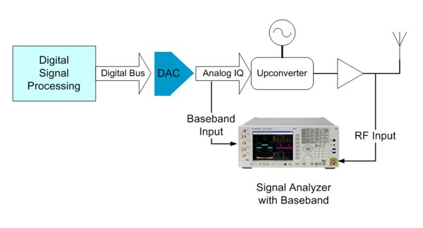 Figure 1b: Separate digital-to-analog converter with analog I/Q upconversion to apply digital modulation on an RF carrier.
Then the analog baseband signals are upconverted to RF using an I/Q modulator-based upconverter.
In this case, a convenient way to analyse the modulation in both baseband and RF domains is with a signal analyser with both baseband and RF inputs.
Analysis engines, such as Agilent 89601A vector signal analysis software, can work with both sets of hardware (logic analyser and the signal analyser, including both the baseband and RF inputs).
Consistent results including views, demodulation algorithms, etc are applied by the software in all cases. Modulation metrics like bandwidth, adjacent channel power (ACPR) or error vector magnitude (EVM) can be evaluated for a variety of modulation formats.
It is important that the baseband inputs of the signal analyser be accurately calibrated. If not, it is impossible to tell if measured impairments are due to the device being evaluated - or in the measurement system itself.
Baseband signals are often measured on printed circuit boards that lack specific output connectors to interface with baseband test instrumentation.
Even if specialised output connectors are provided, it is important to adequately buffer them so that they do not interfere with the main signal chain through the upconverter.
This then raises the question of whether the signal path gain and frequency response through the baseband test port, connector and cable are the same as those through the main signal chain.
Accurate measurements of I/Q modulated signals put severe constraints on test equipment, requiring exceptional accuracy in the complex I/Q channel match.
The BBIQ system uses a high-linearity frontend and a 16-bit ADC for better distortion and dynamic range performance than can be achieved on an oscilloscope.
Any phase delay of the interconnect cables must be calibrated out.
Probing is one way to address some of these interconnection issues, but in this case capacitive loading effects on the circuit should be minimised. In addition, any frequency response variation and time skew in the probes must be characterised and corrected.
This probing process is complicated by having circuit impedances on the PCB that often differ from the 50 Ω impedance of the analyser inputs.
In general what is needed to accurately measure I/Q signals on a PCB is a high-impedance probe that presents minimal capacitive loading to the circuit under test. Devices such as the Agilent InfiniiMax series have been developed for oscilloscopes, with a wide variety of methods of interfacing to the circuit under test.
Both passive and active probes are used. The bandwidth required of the probes for BBIQ (~40 MHz) is typically much less than that needed on modern oscilloscopes (>1 GHz).
However, the amplitude, phase and offset calibration requirements for BBIQ are more severe, necessitated by the difficulties in achieving accurate modulation quality measurements.
Active probes present very low capacitive loading to the circuit, while maintaining wide modulation bandwidth coverage. However, with active probes it is necessary to provide power to the probes, as well as to identify the probe types to ensure adequate matching between the I and Q channels.
As an example, the MXA signal analyser now includes a baseband input option that includes the InfiniiMax probe interface to identify and power these probes.
In addition, the calibration requirements for accurate baseband I/Q measurements are addressed in the MXA calibration software and hardware.
Several of the InfiniiMax probes with the best characteristics for accurate BBIQ measurements are supported by the MXA software.
For example, the 113xA family of active probes (including 1130A 1131A, 1132A, and 1134A) are fully supported on the MXA signal analyser. Differential signals are often used in analog baseband systems to minimise noise and distortion - due to their common mode rejection and comparatively small output voltage swings.
The 113xA probes present a very compact way of directly probing differential signals, as shown in Figure 2. In this case the 1130A probe amplifier is used with the E2675A differential browser accessory.
|
|

The signal analyser has differential inputs on both the I and Q channels for cabled signals (four input BNC connectors). However, when employing the differential active probe, the active probe head converts the differential signal to one single-ended InfiniiMax probe connection to the input BNC.
A pair of differential probes is used, connected to the I and Q inputs of the analyser.
Differential active probes can also be used to probe single-ended signals. In this case, it is possible to provide an adjustable offset voltage at the probe head to compensate for any voltage offset in the signal being measured.
Passive probes present another alternative for probing baseband signals. The 1161A passive probe is fully supported by the signal analyser.
These probes provide a lower cost option, using the 1 MΩ input impedance selection on the MXA BBIQ inputs. To avoid loading the circuit, the probe provides a 10:1 voltage division.
Using the probe ID feature, this attenuation is calibrated out in the measurement. This probe presents a capacitance of ~10 pF to the input device, higher than the active probe but adequate for many applications.
The bandwidth is sufficient to support the full 40 MHz frequency range of both the I and Q inputs (80 MHz of I/Q bandwidth).
However, the passive probes have a more limited range of interface options on the PC board. When probing differential signals, two separate probes are required for each channel.
These are connected on each of the differential input BNC connectors (for example, two probes on the I and I bar inputs for the I channel).
For both active and passive probes, it is necessary to calibrate the probes to obtain accurate measurements. Passive probes must also be compensated before calibration.
Compensation adjusts the high frequency capacitive divider in the probe to match the low frequency resistive divider. This optimises the complex frequency response at the crossover frequency.
Flat frequency response across the crossover is important to minimise amplitude and phase errors at these low frequencies, which can degrade modulation measurements.
The crossover frequency is sufficiently low that the subsequent calibration step cannot correct for it. A BNC output calibrator is provided for both calibration and passive probe compensation.
A square wave from this calibration port is used to manually adjust the compensation capacitor screw on each passive probe to equalise the low frequency and high frequency gains in the time domain. This is done by minimising any undershoot (undercompensation) or overshoot (overcompensation) of the measured square wave.
Users of passive probes on oscilloscopes will be familiar with the compensation procedure, which is similar to that performed on an oscilloscope.
The probe calibration procedure gives a way of accurately measuring the complex gain versus frequency of both input channels and probes using a time domain square wave.
The same procedure can be used for cabled calibration measurements, if probes are not employed. A very high degree of gain matching between channels is required for accuracy in I/Q measurements and digital demodulation.
For example, a constellation measurement of a signal with a 1 dB gain imbalance is shown in Figure 3. Note the non-square appearance of the constellation and the mismatch between the constellation reference targets (circles) and the measured symbol values.
|
|

The result is an increase in EVM to over 5%, a measurement error that could easily hide circuit errors.
Even a small 0.1 dB gain difference between the I and Q channels will result in images of about -45 dB on a single-sideband modulated signal and EVM errors of about 0.5%.
Both these errors are significant in a well-optimised system. Small phase errors due to cable time skew can cause similar issues.
It is also necessary to perform this calibration at all modulation frequencies. Finally, very small DC offsets will result in LO feedthrough in the measured result. These impairments are summarised in Table 1.
|
|

An accurate calibrator signal and supporting analyser software can be used to characterise and correct for all these errors. For directly cabled measurements with the MXA, this calibration can be performed with a short cable connected directly from the calibrator to the input port.
For probes, the complex frequency response of each probe is individually measured and stored in the instrument for later correction of the measured data.
This probe calibration process is detailed to the user with a graphical guided set-up procedure. This is shown in Figure 4, for the example of the 1161A passive probe.
|
|

The probe calibration is typically performed when the probes are first connected. The results should not vary significantly if the temperature varies less than ±5 °C.
Offset calibrations are performed internally to reduce the offset errors that appear as LO feedthrough in the baseband frequency domain measurement.
In summary, accurate modulation quality measurements are helpful, and frequently indispensable in designing and characterising modern digital wireless systems.
Analysing baseband signals as well as RF is needed but baseband analysis presents novel demands on the test engineer. Probing can be helpful in meeting the unique requirements of baseband signal characterisation.
By careful attention to probe calibration techniques, accurate measurements can be obtained.
A signal analyser designed for probing with a specialised graphical user interface, calibration hardware and a variety of convenient probing solutions simplifies this process. Analysis software can then provide accurate, consistent measurements of both RF and baseband signals.
Written by Roger L Jungerman, Agilent Technologies.
Turning RFID tags into scalable passive sensors
Researchers from UC San Diego have used low-cost RFID tags to develop analog passive sensors that...
Smart buoy tech live streams data 24/7 from sea floor
A Perth-based company has developed the Nodestream protocol, a bespoke solution that uses...
Engineers discover a new way to control atomic nuclei as “qubits”
Using lasers, researchers can directly control a property of nuclei called spin, that can encode...


")
