Attosecond boost helps microscope film light and matter

Electron microscopes provide insight into the tiniest details of materials and can visualise, for example, the structure of solids, molecules or nanoparticles with atomic resolution. However, most materials in nature are not static; they constantly interact, move and reshape between initial and final configurations. One of the most general phenomena is the interaction between light and matter, which is omnipresent in materials such as solar cells, displays or lasers. These interactions are defined by electrons pushed and pulled around by the oscillations of light, and the dynamics are fast: light waves oscillate at attoseconds, a billionth of a billionth of a second.
Until now, it has been difficult to directly visualise these fast processes in space and time, but physicists from the University of Konstanz have now succeeded in recording movies with attosecond time resolution in a transmission electron microscope, providing new insights into the functionality of nanomaterials and dielectric meta-atoms. The research findings were published in the scientific journal Nature.
Peter Baum, physics professor at the University of Konstanz, said that almost all phenomena in optics, nanophotonics or metamaterials occur on time scales below one oscillation period of a light wave. To film the ultrafast interactions between light and matter, we therefore need a time resolution of attoseconds,” Baum said.
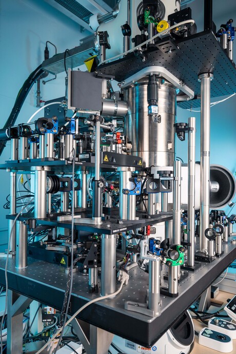
To achieve this recording speed, Baum’s research group used the fast oscillations of a continuous-wave laser to convert the electron beam of an electron microscope into a sequence of ultrashort electron pulses. In this process, a thin silicon membrane creates a periodic acceleration and deceleration of the electrons. David Nabben, first author of the study, said this modulation causes the electrons to catch up with each other. “After some time, they convert into a train of ultrashort pulses,” Nabben said.
Another laser wave creates the interaction with the sample object. The ultrashort electron pulses are then used to measure the object’s response to the laser light, frozen in time like a stroboscope. Ultimately, the researchers obtain a movie of the processes with attosecond time resolution.
In their study, the scientists presented several examples of time-resolved measurements in nanomaterials. The experiments showed the emergence of chiral surface waves that can be controlled by the researchers to travel in a specific spatial direction, or characteristic time delays between different modes of radiation from nanoantennas. The scientists not only investigated such surface phenomena, but also filmed the electromagnetic processes inside a waveguide material.
The results are interesting for further developments in nanophotonics and demonstrate the broad application range of attosecond electron microscopy.
“The direct measurement of the electromagnetic functionality of materials as a function of space and time is not only of great value for fundamental science, but also opens up the way for new developments in photonic integrated circuits or metamaterials,” Nabben said.
Ultra-thin fibre microphone monitors power grid systems
Immune to extreme heat and high voltage, the new device could listen for problems inside...
AI-powered wearable turns gestures into robot commands
A new wearable system uses stretchable electronics and artificial intelligence to interpret human...
Graphene-based solar cells power temperature sensors
Researchers have demonstrated the ultra-low-power temperature sensors powered by graphene-based...


