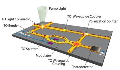
Metamaterials manipulate light on a microchip
Using a combination of the new tools of metamaterials and transformation optics, engineers at Penn State University have developed designs for miniaturised optical devices that can be used in chip-based optical integrated circuits, the equivalent of the integrated electronic circuits that make possible computers and mobile phones.
Controlling light on a microchip could, in the short term, improve optical communications and allow sensing of any substance that interacts with electromagnetic waves. In the medium term, optical integrated circuits for infrared imaging systems are feasible. Further down the road lies high-speed, all-optical computing. The path forward requires some twists on well-known equations and the construction of structures smaller than the wavelength of light.

Light bends naturally as it crosses from one material to another, a phenomenon called refraction that can be seen in the way a stick seems to bend in water. Illusions, such as mirages in the desert or the shimmer of water on the road ahead on a hot day, are caused by a difference in the refractive index of layers of warmer and cooler air. The new field of transformation optics (TO) uses this light-bending phenomenon in a rigorously mathematical way by applying the 150-year-old Maxwell equations describing the propagation of light onto structures known as metamaterials, artificial constructs with custom-designed refractive indexes. The most famous applications of metamaterials are cloaking devices and perfect lenses, but those are just the tip of the optical iceberg.
In a paper in a new online journal, Light: Science and Applications, published by Nature Publishing Group, Douglas Werner, professor of electrical engineering, and his post-doc Qi Wu and PhD student Jeremiah Turpin present a unified theory for designing practical devices on a single platform using transformation optics. “This field [transformation optics] is in its early stages, so there are many contributions to be made,” Werner says. “Our big contribution is in figuring out how to develop TO designs with the simplest material parameters without impacting performance, and linking the devices together to form an on-chip integrated photonic system.”
Among their designs are light collimators, which take light from a source and focus it into one or more tightly focused beams - waveguide couplers, which connect different sized waveguides; TO splitters, which divide power from an input waveguide to two or more output waveguides; waveguide crossings, which route light in compact spaces without loss or crosstalk; and TO benders, which turn the light around corners without loss. These devices are only five to 10 microns in size, and therefore many of them could fit on a centimetre-sized chip.
“It has been a joint effort to develop these transformation optics tools and designs,” Werner says. “Jeremy wrote the algorithms behind the simulation tools. Qi is developing the designs to be simulated. In order to get the best design for a targeted application, thousands of simulations may have to be performed using powerful optimisation techniques developed in our group.”
Transformation optics devices that perform diverse, simple functions can be integrated together to build complex photonic systems for optical communications, imaging, computing and sensing, say the authors. The current, non-TO approach is to design each device using different methods and materials that may not be compatible on a single platform. The Werner group’s technique, on the other hand, employs graded index metamaterial structures, such as patterned air holes or rods, on a silicon-on-insulator platform that can be easily integrated into on-chip photonic systems, providing broad bandwidth and low losses.
In order to keep their designs grounded in reality, the group works closely with nanofabricators at Penn State’s Nanofabrication Laboratory who are themselves developing new approaches to implement the Werner group’s designs. All of the designs described in the paper can be realistically built with current fab processes, says Werner. “It’s like a CAD tool,” he explains, citing the computer-aided design tools used in manufacturing. “We’ve developed customised transformation optics simulation and optimisation tools for designing optical devices. Beyond that,” he continues, “TO is flexible enough that it opens up the possibility of creating all sorts of new devices that don’t currently exist.”
Faster space communication with record-sensitive receiver
Researchers have developed a new system featuring a silent amplifier and a sensitive receiver,...
New record set for wireless data transfer
Researchers from University College London have set a new record for wireless transmission speed,...
Electrically modulated light antennas for faster computer chips
Researchers have achieved electrically controlled modulation of light antennas, paving the way...


