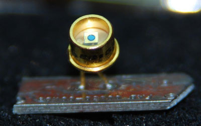
Ultrafast semiconductor devices exploit photoelectric effect

UK and US researchers have developed compound semiconductor (CS) technology that could drive future high-speed data communications, creating an ultrafast and highly sensitive ‘avalanche photodiode’ (APD) that generates less electronic noise than its silicon rivals.
APDs are highly sensitive semiconductor devices that exploit the ‘photoelectric effect’ — when light hits a material — to convert light to electricity. Fast, supersensitive APDs are in demand worldwide for use in high-speed data communications and light detection and ranging (LIDAR) systems for autonomous vehicles.
Now, researchers from Cardiff University’s Institute for Compound Semiconductors (ICS) have partnered with the University of Sheffield and the California NanoSystems Institute at the University of California, Los Angeles (UCLA) to create APDs with low excess noise and high sensitivity. Their work has been described in the journal Nature Photonics.
“The innovation lies in the advanced materials development using molecular beam epitaxy (MBE) to ‘grow’ the compound semiconductor crystal in an atom-by-atom regime,” said Sêr Cymru Professor Diana Huffaker, Scientific Director of ICS. “This particular material is rather complex and challenging to synthesise, as it combines four different atoms requiring a new MBE methodology. The Sêr Cymru MBE facility … is designed specifically to realise an entire family of challenging materials targeting future sensing solutions.”
Dr Shiyu Xie, Sêr Cymru Cofund Fellow, said, “The results we are reporting are significant as they operate in very low-signal environments, at room temperature, and very importantly are compatible with the current InP optoelectronic platform used by most commercial communication vendors.
“These APDs have a wide range of applications. In LIDAR, or 3D laser mapping, they are used to produce high-resolution maps, with applications in geomorphology, seismology and in the control and navigation of some autonomous cars.
“Our findings can change the global field of research in APDs. The material we have developed can be a direct substitute in the current existing APDs, yielding a higher data transmission rate or enabling a much longer transmission distance.”
The Sêr Cymru Group within ICS is now preparing a proposal with collaborators at Sheffield for funding from UK Research and Innovation to support further work, with Prof Huffaker noting, “We are working closely with Airbus and the Compound Semiconductor Applications Catapult to apply this technology to future free space optics communication system.
“Our work … has the potential to yield a new class of high-performance receivers for applications in networking and sensing.”
Please follow us and share on Twitter and Facebook. You can also subscribe for FREE to our weekly newsletter and bimonthly magazine.
Red OLED microdisplay for energy-efficient AR/VR
Researchers have developed a CMOS-based red OLED microdisplay with luminance and improved power...
Next-gen semiconductor material for light-based electronics
Scientists from the University of Edinburgh have created a new type of material that could enable...
Chip-scale optical amplifier enhances data and sensing
Energy-efficient and small enough to fit in a smartphone, an optical amplifier developed at...


