Toshiba develops SiC MOSFET with embedded Schottky barrier diode

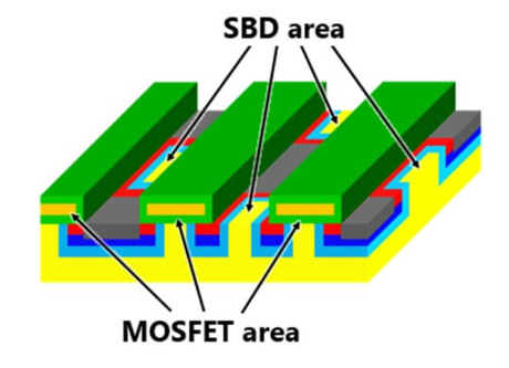
Toshiba Electronic Devices & Storage Corporation and Toshiba Corporation (collectively ‘Toshiba’) have developed a SiC metal oxide semiconductor field effect transistor (MOSFET) that arranges embedded Schottky barrier diodes (SBD) in a check pattern (check-pattern embedded SBD) to realise both low on-resistance and high reliability. Toshiba has confirmed that the design secures an approximately 20% reduction in on-resistance (RonA) against its current SiC MOSFET, with no loss of reliability. On-resistance is the resistance value between the drain and source of a MOSFET during operation (ON).
Power devices are essential components for managing electric energy and reducing power loss in all kinds of electronic equipment. SiC has the potential to be the next-generation material for power devices, as it delivers higher voltages and lower losses than silicon. While use of SiC is limited to inverters for trains, wider applications are on the horizon, in areas including vehicle electrification and the miniaturisation of industrial equipment. However, bipolar conduction in the body diode during reverse operation of SiC MOSFET can be harmful as it degrades on-resistance.
Toshiba Electronic Devices & Storage Corporation developed a device structure that embeds SBDs into the MOSFET to inactivate body diodes, but found that replacing the MOSFET channel with an embedded SBD lowers channel density and increases RonA. This trade-off has been resolved with a new embedded SBD structure, with Toshiba confirming that it also improves performance characteristics. Toshiba has improved both conduction loss in its SBD-embedded SiC MOSFET and achieved good diode conductivity by deploying a check-pattern SBD distribution. Evaluation of the on-side current characteristics of 1.2 kV-class-SBD-embedded MOSFETS with the optimised design confirmed that using the check design to position the embedded-SBDs close to the body diodes effectively limits bipolar conduction of the parasitic diodes, while the unipolar current limit of reverse conduction is double that realised by the current striped SBD pattern design for the same SBD area consumption. RonA was found to be approximately 20% lower, at 2.7mΩ・cm2.
This confirmed improvement in the trade-off is essential if SiC MOSFETs are to be used in inverters for motor drive applications. Toshiba will continue carrying out evaluations toward improving dynamic characteristics and reliability, and to develop high-performance power semiconductors that contribute to carbon neutrality.
3D semiconductor chip alignment boosts performance
Researchers have developed an ultra-precise method to align 3D semiconductor chips using lasers...
Researchers achieve 8 W output from optical parametric oscillator
Researchers have demonstrated a total output power of 8 W from a high-power mid-infrared cadmium...
"Dualtronic" chip for integrated electronics and photonics
Cornell researchers have developed a dual-sided chip known as a "dualtronic" chip that...


