Thanks for the memristors

In the race to build a computer that mimics the massive computational power of the human brain, researchers are increasingly turning to memristors, which can vary their electrical resistance based on the memory of past activity. Now, scientists at the National Institute of Standards and Technology (NIST) in the US have unveiled the inner workings of these semiconductor elements, which can act like the short-term memory of nerve cells.
Just as the ability of one nerve cell to signal another depends on how often the cells have communicated in the recent past, the resistance of a memristor depends on the amount of current that recently flowed through it. Moreover, a memristor retains that memory even when electrical power is switched off.
But despite the interest in memristors, scientists have lacked a detailed understanding of how these devices work and have yet to develop a standard toolset to study them. The NIST scientists have now identified such a toolset and used it to more deeply probe how memristors operate, with the results published in the journal Nature Communications.
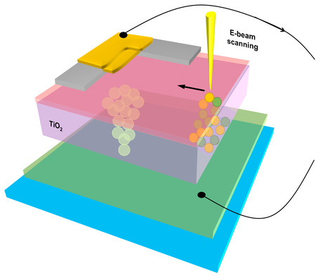
To explore the electrical function of memristors, the team aimed a tightly focused beam of electrons at different locations on a titanium dioxide memristor. The beam knocked free some of the device’s electrons, which formed ultrasharp images of those locations. The beam also induced four distinct currents to flow within the device. The team determined that the currents are associated with the multiple interfaces between materials in the memristor, which consists of two metal (conducting) layers separated by an insulator.
“We know exactly where each of the currents are coming from because we are controlling the location of the beam that is inducing those currents,” said study co-author Brian Hoskins.
In imaging the device, the team found several dark spots — regions of enhanced conductivity — which indicated places where current might leak out of the memristor during its normal operation. These leakage pathways resided outside the memristor’s core — where it switches between the low and high resistance levels that are useful in an electronic device.
The finding suggests that reducing the size of a memristor could minimise or even eliminate some of the unwanted current pathways. Although researchers had suspected that might be the case, they had lacked experimental guidance about just how much to reduce the size of the device. And because the leakage pathways are tiny, involving distances of only 100 to 300 nm, “you’re probably not going to start seeing some really big improvements until you reduce dimensions of the memristor on that scale”, Hoskins said.
The team also found that the current that correlated with the memristor’s switch in resistance didn’t come from the active switching material at all, but the metal layer above it. Taken with their other findings, this has led the team to state that “you can’t just worry about the resistive switch, the switching spot itself — you have to worry about everything around it”, said Hoskins.
3D semiconductor chip alignment boosts performance
Researchers have developed an ultra-precise method to align 3D semiconductor chips using lasers...
Researchers achieve 8 W output from optical parametric oscillator
Researchers have demonstrated a total output power of 8 W from a high-power mid-infrared cadmium...
"Dualtronic" chip for integrated electronics and photonics
Cornell researchers have developed a dual-sided chip known as a "dualtronic" chip that...


