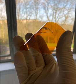
Semiconductor nanowires embedded into flexible surfaces

Engineers from the University of Glasgow have, for the first time, affordably ‘printed’ high-mobility semiconductor nanowires onto flexible surfaces to develop high-performance, ultrathin electronic layers. These surfaces, which can be bent, flexed and twisted, could lay the foundations for a wide range of bendable electronics including video screens, health monitoring devices, implantable devices and synthetic skin for prosthetics.
The work is the latest development from the university’s Bendable Electronics and Sensing Technologies (BEST) research group, led by Professor Ravinder Dahiya. The BEST team has already developed innovative technologies including solar-powered ‘electronic skin’ for use in prosthetics, stretchable sensors which can monitor the pH levels of users’ sweat and most recently, a graphene supercapacitor which could be used in the next generation of wearable health sensors.
Writing in the journal Microsystems and Nanoengineering, the research team outlined how they manufactured semiconductor nanowires from both silicon and zinc oxide and printed them on flexible substrates to develop electronic devices and circuits. In the process, they discovered that they could produce uniform silicon nanowires which aligned in the same direction, as opposed to the more random, tree branch-like arrangement produced by a similar process for zinc oxide. Since electronic devices run faster when electrons can run in straight lines as opposed to having to negotiate twists and turns, the silicon nanowires were best suited to use in their flexible surfaces.
From there, the team engaged in a series of experiments to print the wires into flexible surfaces with a printing device they developed and built in their lab. After a series of experiments, they were able to find the optimal combination of pressure and velocity to effectively print the nanowires time after time.
“This paper marks a really important milestone on the road to a new generation of flexible and printed electronics,” Professor Dahiya said. “In order for future electronic devices to integrate flexibility into their design, industry needs to have access to energy-efficient, high-performance electronics which can be produced affordably and over large surface areas.
“With this development, we’ve gone a long way to hitting all of those marks. We’ve created a contact-printing system which allows us to reliably create flexible electronics with a high degree of reproducibility, which is a really exciting step towards creating all kinds of bendable, flexible, twistable new devices.
“We’ve just secured further funding which we’ll use to scale up the process further, making it more readily applicable to industrial purposes, and we’re looking forward to building on what we’ve managed to achieve already.”
Single transistor used to implement neuromorphic behaviour
Researchers have demonstrated that a single transistor can mimic neural and synaptic behaviours,...
Novel fabrication technique for flexible electronics
Researchers have harnessed nature's intrinsic hierarchical fractal structures to improve the...
Novel antenna tech developed for 6G communications
Researchers have developed a novel metasurface antenna that can generate and control multiple...


