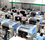
Oxide growth system for next-gen semiconductors

Researchers at the Israel Institute of Technology have demonstrated control over an emerging material, which could be used as a future alternative to silicon in microelectronics. Integrated circuits, commonly known as computer chips, are responsible for processing, storing and transferring large quantities of data. The continuous performance improvement of these chips is driven by shrinking the size of the transistor.
Transistors are miniature switches that control the flow of electric currents. Professor Lior Kornblum from the Erna Viterbi Faculty of Electrical and Computer Engineering at the Israel Institute of Technology said that as a result of the continuous miniaturisation, modern transistors are only a few dozen atoms across — because they are so small, continuing miniaturisation without compromising their performance is becoming increasingly challenging. “On the nanometric scale, the transistors behave in new ways that are different than their larger predecessors,” Kornblum said.
One manifestation of this problem is leakage of electric current when the transistor (switch) is supposed to be off. Kornblum said that the problem can be compared to a leaking faucet. “In a modern phone with billions of transistors, the tiniest current leakage will accumulate into a considerable waste of energy. This could quickly drain the battery and cause excessive heating of the device. Zooming out, when thinking server farms and data centres, the energy waste can be substantial and produce considerable heat,” Kornblum said.
Kornblum’s research group is studying silicon to tackle these challenges. The researchers analysed various oxide materials, one of which can switch from being an electrical conductor to an insulator — and back. The researchers want to harness this property for future transistors that could potentially switch more efficiently. Developing such technology requires precise control of the material properties. The researchers demonstrated a route for manipulating the materials’ electric properties by controlling the distance between its atoms. Laboratory manager Dr Maria Baskin achieved this by using a unique oxide growth system; she deposited layers of atoms one on top of the other, thereby growing films of the material. She was able to set the distances between atoms with picometre (one-thousandth of a nanometre) precision.
This oxide growth system enabled the development of the next generation of semiconductors, magnetic materials and renewable energy materials such as cutting-edge catalysts. “We can choose from a variety of atoms, control their arrangement and the spacing between them. Using these capabilities, we can even create materials that did not exist before, with a broad range of properties per our requirements,” Baskin said.
Kornblum said the tools the researchers developed for the oxides growth are unique. “Oxide growth is only the first step. From there, the graduate students start their research. Some focus on the materials’ physical properties, striving to understand how they function, and some utilise these materials to fabricate electronic devices that we hope will revolutionise microelectronics, renewable energy and other fields,” Kornblum said.
PhD student Lishai Shoham’s research studies the material’s properties and fabricates transistors from it, to evaluate how it can be harnessed for microelectronics. Shoham’s research showed that by stretching the material at the atomic level, the elongation of the chemical bonds between the atoms changes the electrical properties: stretching by less than 2% of the atomic bond length, the researchers reduced the electrons’ tendency to hop from atom to atom. The stretching also changed how the atoms were arranged in space; through these tiny changes, which took place at a scale of one picometre, the researchers developed the groundwork for controlling the material’s transition from a conducting state to an insulating state.
Red OLED microdisplay for energy-efficient AR/VR
Researchers have developed a CMOS-based red OLED microdisplay with luminance and improved power...
Next-gen semiconductor material for light-based electronics
Scientists from the University of Edinburgh have created a new type of material that could enable...
Chip-scale optical amplifier enhances data and sensing
Energy-efficient and small enough to fit in a smartphone, an optical amplifier developed at...


