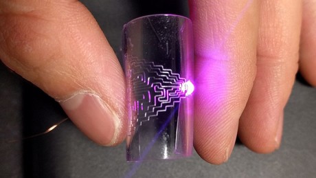
Making flexible electronics with metal printing

US researchers have developed a new technique for directly printing metal circuits, creating flexible, stretchable electronics. Described in the journal Advanced Materials Technologies, the technique can use multiple metals and substrates and is compatible with existing manufacturing systems that employ direct printing technologies.
“Flexible electronics hold promise for use in many fields, but there are significant manufacturing costs involved — which poses a challenge in making them practical for commercial use,” said Jingyan Dong, an associate professor at North Carolina State University and corresponding author on the study.
“Our approach should reduce cost and offer an efficient means of producing circuits with high resolution, making them viable for integrating into commercial devices.”
The technique uses existing electrohydrodynamic printing technology, which is already used in many manufacturing processes that use functional inks. But instead of ink, Dong’s team uses molten metal alloys with melting points as low as 60°C. The researchers have demonstrated their technique using three different alloys, printing on four different substrates: one glass, one paper and two stretchable polymers.
“This is direct printing,” said Dong. “There is no mask, no etching and no moulds, making the process much more straightforward.”
The researchers tested the resilience of the circuits on a polymer substrate and found that the circuit’s conductivity was unaffected even after being bent 1000 times. The circuits were still electrically stable even when stretched to 70% of tensile strain.
The researchers also found that the circuits are capable of ‘healing’ themselves if they are broken by being bent or stretched too far. As explained by Dong, “Because of the low melting point, you can simply heat the affected area up to around 70°C and the metal flows back together, repairing the relevant damage.”
The researchers demonstrated the functionality of the printing technique by creating a high-density touch sensor, fitting a 400-pixel array into one square centimetre. According to Dong, they are now open to working with industry “to implement the technique in manufacturing wearable sensors or other electronic devices”.
AI workflow accelerates semiconductor materials discovery
Researchers from the University of New South Wales have developed an AI-driven system to...
Monash reveals atomic switching in new memory tech
Researchers have captured atomic motion behind memory switching, revealing how data is written...
Red OLED microdisplay for energy-efficient AR/VR
Researchers have developed a CMOS-based red OLED microdisplay with luminance and improved power...


