Boosting light absorption in thin silicon photodetectors

Photonic systems are gaining traction in many emerging applications, including optical communications, lidar sensing, and medical imaging. However, widespread adoption of photonics in future engineering solutions relies on the cost of manufacturing photodetectors, which depends on the kind of semiconductor utilised for the purpose. Traditionally, silicon (Si) has been the most prevalent semiconductor in the electronics industry; however, it has a relatively weak light absorption coefficient in the near-infrared (NIR) spectrum compared to those of other semiconductors such as gallium arsenide (GaAs). Because of this, GaAs alloys are suitable for photonic applications, but are incompatible with the traditional complementary metal-oxide semiconductor (CMOS) processes used in the production of most electronics.
Now, a research team from UC Davis in California has developed a strategy to boost the light absorption of thin Si films. In a paper published in Advanced Photonics Nexus, they presented an experimental demonstration of Si-based photodetectors with light-trapping micro- and nano-surface structures, achieving high performance gains that rival those of GaAs and other group III-V semiconductors.
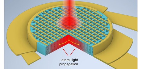
The proposed photodetectors consist of a micrometre-thick cylindrical Si slab placed over an insulating substrate, with metallic ‘fingers’ extending from the contact metals atop the slab in an interdigitated fashion. The bulk Si is filled with circular holes arranged in a periodic pattern that act as photon-trapping sites. The overall structure of the device causes normally incident light to bend by almost 90° upon hitting the surface, making it travel laterally along the Si plane. These laterally propagating modes increase the propagation length of light and slow it down, leading to more light–matter interaction and a consequent increase in absorption.
The researchers conducted optical simulations and theoretical analyses to better understand the effects of the photon-trapping structures, and performed experiments comparing photodetectors with and without them. They found that photon trapping led to an increase in the absorption efficiency over a wide band in the NIR spectrum, staying above 68% and peaking at 86%. The observed absorption coefficient of the photon-trapping photodetector was several times higher than that of plain Si and exceeded that of GaAs in the NIR band.
The research findings demonstrate a promising strategy to boost the performance of Si-based photodetectors for emerging photonics applications. By achieving high absorption in ultrathin Si layers, the parasitic capacitance of the circuit can be kept low, which is crucial for high-speed systems. The proposed approach is also compatible with modern CMOS manufacturing processes and can enhance how optoelectronics are integrated into conventional circuits. This, in turn, could pave the way for affordable ultrafast computer networks and advances in imaging technology.
Single transistor used to implement neuromorphic behaviour
Researchers have demonstrated that a single transistor can mimic neural and synaptic behaviours,...
Novel fabrication technique for flexible electronics
Researchers have harnessed nature's intrinsic hierarchical fractal structures to improve the...
Novel antenna tech developed for 6G communications
Researchers have developed a novel metasurface antenna that can generate and control multiple...


