Atomically thin nanoribbons can be produced at scale

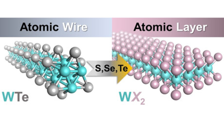
Researchers from Tokyo Metropolitan University (TMU) have used nanowires made of a transition-metal chalcogenide to make atomically thin nanoribbons, which are highly sought after for sophisticated electronic devices. Given the scalability of their method, the researchers hope it will see widespread use in the industrial production of cutting-edge materials.
As electronic circuitry gets smaller, faster and more energy-efficient, scientists are faced with the increasingly difficult challenge of controlling the atomic-level structure of the materials that are used inside it. One promising avenue of research is the use of intricate threads of material only a few atoms wide; one such structure is composed of transition-metal chalcogenides, a combination of transition metals and chalcogens — atoms which share a column with oxygen on the periodic table.
These atomically thin nanowires possess properties that are apparently unique to their one-dimensional structure and are highly sought after for sophisticated electronic devices. But what they have in minuteness, they lack in tunability. This is where nanoribbons — narrow, atomically thin sheets — come in handy; fine control of their width, for example, leads to controlled variation in their electronic and magnetic properties.
A great deal of work has been applied to ‘build’ nanoribbons from the bottom up. But such methods aren’t very scalable, which is a problem for producing bulk quantities for commercial devices. Now TMU researchers have come up with a scalable way of assembling nanowires into nanoribbons, which they have published in the journal ACS Applied Nano Materials.
The team had already pioneered ways to produce nanowires in bulk quantities. By taking some tungsten telluride nanowires, they created bundles of wires deposited on a flat substrate. These were exposed to vapours of different chalcogens like sulfur, selenium and tellurium. With a combination of heat and vapour, the initially separate threads in the bundles were successfully woven together into narrow, atomically thin nanoribbons with a characteristic zigzag structure.
By tuning the thickness of the original bundles, the team could choose whether these ribbons were oriented parallel to the substrate or perpendicular to it. Furthermore, by tuning the substrate on which the bundles are placed, they could control whether the ribbons were randomly oriented or pointing in a single direction. Importantly, the method is scalable and may be applied to take the synthesis from lab-scale manufacture of a few ribbons to bulk syntheses over large substrate areas.
The team were able to confirm that the ribbons they created had the exotic electronic properties which are unique to their one-dimensional nature. Their research thus provides a big leap forward for materials science, as well as a tangible step towards seeing mass-produced nanoribbons in state-of-the-art electronics, optoelectronics and catalysts.
Please follow us and share on Twitter and Facebook. You can also subscribe for FREE to our weekly newsletter and bimonthly magazine.
A lighter, smarter magnetoreceptive electronic skin
Researchers have developed an innovative e-skin that facilitates a new level of interaction...
Single transistor used to implement neuromorphic behaviour
Researchers have demonstrated that a single transistor can mimic neural and synaptic behaviours,...
Novel fabrication technique for flexible electronics
Researchers have harnessed nature's intrinsic hierarchical fractal structures to improve the...


