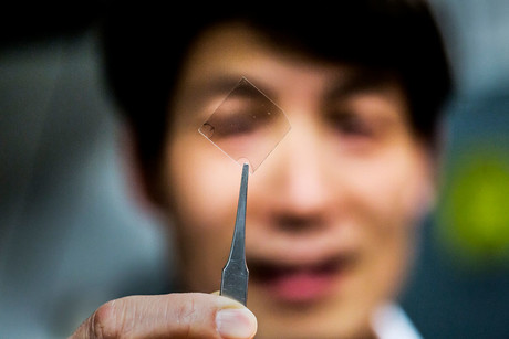
Ultrathin silver films for tarnish-proof touch screens

The thinnest, smoothest layer of silver that can survive air exposure has been developed by a research team led by the University of Michigan (U-M) — and it could change the way touch screens and flat or flexible displays are made.
Screens of all types need transparent electrodes to control which pixels are lit up, but touch screens are particularly dependent on them. A modern touch screen is made of a transparent conductive layer covered with a non-conductive layer. It senses electrical changes where a conductive object — such as a finger — is pressed against the screen.
“The transparent conductor market has been dominated to this day by one single material,” said L Jay Guo, a professor of electrical engineering and computer science at U-M.
This material, indium tin oxide, is projected to become expensive as demand for touch screens continues to grow, as there are relatively few known sources of indium. “Before, it was very cheap,” said Guo. “Now, the price is rising sharply.”
Guo and his team considered silver as a possible successor to this material; unfortunately, it is usually impossible to make a continuous layer of silver less than 15 nm thick. Furthermore, silver has a tendency to cluster together in small islands rather than extend into an even coating, Guo noted.
By combining the silver with about 6% aluminium, the researchers found that it was possible to coax the metal into a film of only 7 nm. They also applied an anti-reflective coating to make one thin metal layer up to 92.4% transparent. Their study results were published in the journal Advanced Materials.
When the scientists exposed their material to air, it didn’t immediately tarnish as pure silver films do. After several months, the film maintained its conductive properties and transparency. It was also firmly stuck on, whereas pure silver comes off glass with Scotch tape.
In addition to its potential to serve as a transparent conductor for touch screens, silver has an unparalleled ability to transport visible and infrared light waves along its surface. The light waves shrink and travel as so-called surface plasmon polaritons, showing up as oscillations in the concentration of electrons on the silver’s surface. Those oscillations encode the frequency of the light, preserving it so that it can emerge on the other side.
While optical fibres can’t scale down to the size of copper wires on today’s computer chips, plasmonic waveguides could allow information to travel in optical rather than electronic form for faster data transfer. As a waveguide, the smooth silver film could transport the surface plasmons over a centimetre — enough to get by inside a computer chip.
The plasmonic capability of the silver film can also be harnessed in metamaterials, which handle light in ways that break the usual rules of optics. Because the light travels with a much shorter wavelength as it moves along the metal surface, the film alone acts as a superlens. Or, to make out even smaller features, the thin silver layers can be alternated with a dielectric material, such as glass, to make a hyperlens. Such lenses can image objects that are smaller than the wavelength of light, which would blur in an optical microscope, and can additionally enable laser patterning to achieve smaller features.
The study was supported by the National Science Foundation and the Beijing Institute of Collaborative Innovation. U-M has applied for a patent and is now seeking partners to bring the technology to market.
Spinning, twisted light could power next-generation electronics
Researchers have created an organic semiconductor that forces electrons to move in a spiral...
Improving the way flash memory is made
Researchers are developing the ideal manufacturing process for a type of digital memory known as...
Optical memory unit boosts processing speed
Researchers have developed a fast, versatile volatile photonic memory that could enhance AI,...


