Star-spangled nanowires

US researchers have described a material that, when heated by several hundred degrees, transforms from an atomically thin, two-dimensional sheet into an array of one-dimensional nanowires, each just a few atoms wide. Their discovery has been published in the journal Advanced Materials.
For several years, the team at The University of Texas at Dallas had been searching for a material whose electrical properties might make it suitable for small, energy-efficient transistors to power next-generation electronic devices. In some cases, these properties may only arise once a material has been subjected to a change in external conditions, as part of a process called a phase transition. A change in external temperature and pressure may cause a material’s atoms to rearrange and redistribute to make a material with a different structure and different composition — and different properties.
Using a transmission electron microscope, Dr Moon Kim and his colleagues observed 2D sheets of molybdenum ditelluride, a material made up of one layer of molybdenum atoms and two layers of tellurium atoms. The material belongs to a class called transition metal dichalcogenides (TMDs), which show promise in replacing silicon in transistors.
“We wanted to understand the thermal stability of this particular material,” Dr Kim said. “We thought it was a good candidate for next-generation nanoelectronics. Out of curiosity, we set out to see whether it would be stable above room temperature.”
When they increased the temperature to above 450°C, two things happened.
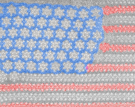
“First, we saw a new pattern begin to emerge that was aesthetically pleasing to the eye,” Dr Kim said. Across the surface of the sample, the repeating rows, or stripes, of molybdenum ditelluride layers began to transform into shapes that looked like tiny six-pointed stars, or flowers with six petals.
The material was transitioning into hexa-molybdenum hexa-telluride, a one-dimensional wire-like structure. The cross-section of the new material is a structure consisting of six central atoms of molybdenum surrounded by six atoms of tellurium.
As the phase transition progressed, part of the sample was still ‘stripes’ and part had become ‘stars’ — a pattern that resembled the United States flag. The researchers even made a false-colour version with a blue field behind the stars and half of the stripes coloured red, to make a ‘nanoflag’.
“Then, when we examined the material more closely, we found that the transition we were seeing from ‘stripes’ to ‘stars’ was not in any of the phase diagrams,” Dr Kim said, referring to a type of graphic that helps researchers predict structural and property changes in materials. “Normally, when you heat up particular materials, you expect to see a different kind of material emerge as predicted by a phase diagram. But in this case, something unusual happened — it formed a whole new phase.”
Each individual nanowire, smaller than 1 nm in diameter, was found to be a semiconductor, which means that electric current moving through the wire could be switched on and off, Dr Kim said. These nanowires could therefore be used as switching devices, just as silicon is used in today’s transistors to turn electric current on and off in electronic devices.
“These nanowires are about 10 times smaller than the smallest silicon wires, and, if used in future technology, would result in powerful energy-efficient devices,” Dr Kim said.
The researchers further found that when many of the individual nanowires were grouped together in bulk they behaved more like a metal, which easily conducts current. However, Dr Kim said the researchers would want to use them “one at a time, because we are pushing the size of a transistor as small as possible”.
“Before we can put this discovery to use and make an actual device, we have many more studies to do, including determining how to separate out the individual nanowires, and overcoming technical challenges to manufacturing and mass production,” he said. “But this is a start.”
Spinning, twisted light could power next-generation electronics
Researchers have created an organic semiconductor that forces electrons to move in a spiral...
Improving the way flash memory is made
Researchers are developing the ideal manufacturing process for a type of digital memory known as...
Optical memory unit boosts processing speed
Researchers have developed a fast, versatile volatile photonic memory that could enhance AI,...


