Organic field-effect transistors successfully miniaturised

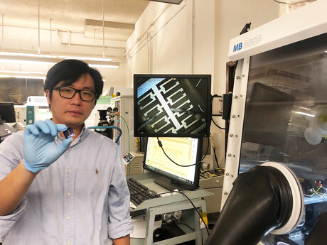
Engineers from The University of Hong Kong (HKU) have developed a monolayer organic semiconductor layer for organic field-effect transistors (OFETs), enabling the transistors to be reduced in size without downgrading their performance. Their work has been described in the journal Advanced Materials.
Field-effect transistors (FET) are the core building blocks of modern electronics such as integrated circuits, computer CPUs and display backplanes. Organic field-effect transistors, which use an organic semiconductor as a channel for current flows, have the advantage of being flexible when compared with their inorganic counterparts like silicon. Other benefits include high sensitivity, biocompatibility, property tunability and low-cost fabrication, giving OFETs great potential in areas such as wearable electronics, conformal health monitoring sensors, bendable displays etc. Potential applications include TV screens that can be rolled up; smart wearable electronic devices and clothing worn close to the body to collect vital body signals for instant biofeedback; and mini-robots made of harmless organic materials working inside the body for diseases diagnosis, mini-surgeries and other treatments.
Until now, the main limitation on enhanced performance and mass production of OFETs has been the difficulty in miniaturising them, as the performance of the transistor will drop significantly with a reduction in size. If the contact resistance of an OFET is large, the transistor channel is patterned to be shorter, and most of the applied voltage will be dissipated in the contact rather than the channel. The OFET properties will then be dominated by two contacts and behave like two back-to-back connected diodes rather than a proper functioning transistor.
Now HKU engineers led by Dr Paddy Chan have developed staggered structure monolayer OFETs, which have apparently demonstrated a record-low normalised contact resistance of 40 Ω·cm. Compared with conventional devices with a contact resistance of 1000 Ω·cm, the device can save 96% of power dissipation at contact when running the device at the same current level. Apart from energy saving, the excessive heat generated in the system — a common problem which causes semiconductors to fail — can be greatly reduced.

“We can further reduce the dimensions of OFETs and push them to a sub-micrometre scale, a level compatible with their inorganic counterparts, while [they] can still function effectively to exhibit their unique organic properties,” Dr Chan said. “This is critical for meeting the requirement for commercialisation of related research.
“If flexible OFETs work, many traditional rigid-based electronics such as display panels, computers and cell phones would transform to become flexible and foldable. These future devices would be much lighter in weight, and with low production cost.
“Moreover, given their organic nature, they are more likely to be biocompatible for advanced medical applications such as sensors in tracking brain activities or neural spike sensing, and in precision diagnosis of brain-related illness such as epilepsy.”

With a US patent having been filed for the innovation, Dr Chan’s team is now working with researchers at HKU and the City University of Hong Kong (CityU) to integrate the miniaturised OFETs into a flexible circuit onto a polymer microprobe for neural spike detection in a mouse brain under different external stimulations. They also plan to integrate the OFETs onto surgical tools such as catheter tubes, and then use it to locate abnormal activity in animal brains.
“Our OFETs provide a much better signal-to-noise ratio,” Dr Chan said. “Therefore, we expect we can pick up some weak signals which cannot be detected before using the conventional bare electrode for sensing.
“We believe that the … OFETs are now ready for applications in large-area display backplanes and surgical tools.”
Please follow us and share on Twitter and Facebook. You can also subscribe for FREE to our weekly newsletter and bimonthly magazine.
Spinning, twisted light could power next-generation electronics
Researchers have created an organic semiconductor that forces electrons to move in a spiral...
Improving the way flash memory is made
Researchers are developing the ideal manufacturing process for a type of digital memory known as...
Optical memory unit boosts processing speed
Researchers have developed a fast, versatile volatile photonic memory that could enhance AI,...


