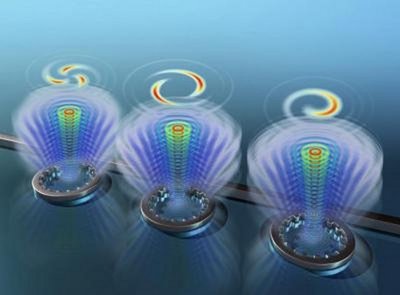
Optical vortices on a chip
An international research group led by scientists from the University of Bristol and the University of Glasgow (UK) and Sun Yat-sen and Fudan universities in China has demonstrated integrated arrays of emitters of so-called “optical vortex beams” onto a silicon chip.
Contradicting traditional conception, light in such beams does not propagate in straight rays. Instead, its energy travels in a spiral fashion in a hollow conical beam shape. The beams therefore look very much like a vortex or cyclone, with its light rays ‘twisted’ either left-handed or right-handed. In theory, there is no limit to how twisted the light rays can be.

In quantum mechanics, this feature is associated with the orbital angular momentum (OAM) of photons - photons in such beams can be thought to orbit around the beam axis, somewhat similar to the movement of planets around the Sun or electrons around a nucleus.
When such light interacts with matter, it asserts a rotational force (a torque) on the matter; therefore, it can be used as so-called “optical spanners” in addition to “optical tweezers”, which can rotate as well as trap microscopic particles or droplets. Different degrees of twist can also be used to transmit information - allowing more information to be carried by a single optical signal and increasing the capacity of optical communications links.
Light beams at the same frequency but with different OAM values can be used to transmit different streams information. Single particles of light (photons) can use these different degrees of twist to represent quantum information, where a single photon can be twisting both clockwise and anticlockwise at the same time. Applications are also being developed in using such light for imaging and sensing purposes. For example, some molecules are chiral - they look the same under normal optical microscopes until illuminated by optical vortex beams with different degrees or directions of twist.
Conventionally, the generation of such beams relied on bulk optical elements such as plates, lenses and holograms. These are good for research but can be inconvenient for many applications, in particular where large numbers of such beams are needed at high packing density.
In contrast, the new emitters invented at Bristol are only a few micrometres in size and thousands of times smaller than conventional elements. They are based on silicon optical waveguides and can be made using standard integrated circuit fabrication technologies.
Siyuan Yu, Professor of Photonics Information Systems in the Photonics Research Group at the University of Bristol, who led the research, said: “Our microscopic optical vortex devices are so small and compact that silicon microchips containing thousands of emitters could be fabricated at very low costs and in high volume.
“Such integrated devices and systems could open up entirely new applications of optical vortex beams previously unattainable using bulk optics.”
These devices are readily interconnected with each other to form complex and large arrays in photonic integrated circuits and could be used for applications including communications, sensing and microscopic particle manipulation.
Dr Mark Thompson, Deputy Director of the Centre for Quantum Photonics at the University of Bristol, added: “Perhaps one of the most exciting applications is the control of twisted light at the single photon level, enabling us to exploit the quantum mechanical properties of optical vortices for future applications in quantum communications and quantum computation.”
The work is featured on the cover of the 19 October 2012 issue of Science magazine.
3D-printed, shape-shifting antenna inspired by sci-fi
Researchers at the Johns Hopkins Applied Physics Laboratory in Laurel, Maryland, have created an...
Researchers knit 'blanket' of radio-frequency antennas
Researchers have used traditional flat-knitting techniques to fabricate flexible and lightweight...
Unlocking next-gen chip efficiency
By studying how heat moves through ultra-thin metal layers, researchers have provided a...


