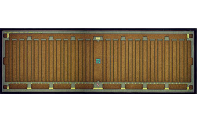
High-frequency transistors said to achieve record efficiency

Researchers at the Fraunhofer Institute for Applied Solid State Physics IAF have significantly increased the output power of their high-frequency transistors for the frequency range from 1 to 2 GHz, doubling the operating voltage of the devices from 50 to 100 V and thus achieving a power-added efficiency of 77.3%.
The team’s technology allows the development of highly efficient amplifiers with even higher power, as required for applications in the fields of plasma generation, industrial heating, communications and radar technologies. Their results were presented at the IEEE International Electron Devices Meeting (IEDM) in San Francisco in December 2019.
The power density of transistors is one of the most important criteria for their use in high-power applications in the GHz range. It determines the size of amplifier modules and thus the system complexity — both of which are decisive for the manufacturing costs and the required use of resources.
There are several ways to increase the power density of transistors, with the Fraunhofer researchers choosing to increase the operating voltage. By scaling the transistor design vertically and laterally, they succeeded in realising high-frequency transistors suitable for applications at an operating voltage of 100 V. These devices, based on the semiconductor gallium nitride (GaN), are characterised by significantly increased power density at frequencies in the GHz range.
Measurements showed a power density of more than 17 W/mm and a power-added efficiency (PAE) of 77.3% at a frequency of 1 GHz — believed to be the highest PAE achieved for 100 V operation in this frequency range ever reported. Tests have also shown that the technology delivers a power density in excess of 20 W/mm at 125 V.
“Increasing the operating voltage from 50 to 100 V enables higher power densities,” said Fraunhofer IAF’s Sebastian Krause, one of the main developers of the technology. “This means that a system can deliver more power on the same area than what is possible with commercially available 50 V or 65 V technologies.”
On the one hand, this enables systems of the same size with higher output power. On the other hand, it is possible to create more compact and lighter systems delivering the same power, since less chip area is required to achieve the desired power level.
“By doubling the operating voltage to 100 V, the transistor exhibits a four times higher output impedance for a given power,” said Krause. This allows the implementation of smaller and therefore less lossy matching networks, which in turn results in higher energy efficiency of the overall system.
“The long-term goal of our development is operation through 10 GHz,” Krause said. This would be of particular interest for high-performance applications such as particle accelerators, mobile phone amplifiers, pulse- and continuous-wave radar, and amplifiers for plasma generators. These systems require high output power levels while maintaining a preferably small footprint — exactly what the 100 V technology can deliver.
Another large industrial field of application is power generators for microwave heating. For a long time, tube-based components (eg, travelling wave tubes) have dominated electronic systems with high output power. However, development is moving towards power semiconductors. The Fraunhofer scientists believe that the GaN-based 100 V technology can provide an efficient alternative for increasing the power of microwave generators.
“In this field, industry usually works at higher frequencies, but vacuum components, eg, magnetrons or klystrons, are predominantly used to date,” Krause commented. “Here, we are working on providing a semiconductor-based alternative. Semiconductors are much more compact and more lightweight, which enables arrangements such as phased arrays.”
Please follow us and share on Twitter and Facebook. You can also subscribe for FREE to our weekly newsletter and bimonthly magazine.
Spinning, twisted light could power next-generation electronics
Researchers have created an organic semiconductor that forces electrons to move in a spiral...
Improving the way flash memory is made
Researchers are developing the ideal manufacturing process for a type of digital memory known as...
Optical memory unit boosts processing speed
Researchers have developed a fast, versatile volatile photonic memory that could enhance AI,...


