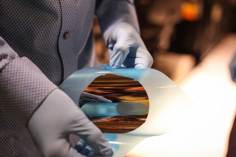
Graphene 'copy machine' to produce cheaper wafers

MIT engineers have developed a technique that could vastly reduce the overall cost of wafer technology for the semiconductor industry, enabling devices made from more exotic, higher-performing materials than conventional silicon.
In 2016, the semiconductor industry spent about $7.2 billion on wafers that serve as the substrates for microelectronics components, which can be turned into transistors, light-emitting diodes and other electronic and photonic devices. Unfortunately, once a wafer’s crystalline pattern is transferred in conventional semiconductor manufacturing, it is so strongly bonded to the semiconductor that it is almost impossible to separate without damaging both layers.
“You end up having to sacrifice the wafer — it becomes part of the device,” said Jeehwan Kim, an associate professor at MIT.
Looking to avoid this, Kim and his team hit on the idea of using a graphene sheet as a sort of ‘copy machine’ to transfer intricate crystalline patterns from an underlying semiconductor wafer to a top layer of identical material. Kim explained that graphene had ideal properties for this task due to the fact that it is robust and ultrathin, with slippery, Teflon-like properties. It could therefore be used by manufacturers as an intermediate layer, said Kim, allowing them to copy and paste a wafer, separate a copied film from the wafer and re-use the wafer many times over.
Testing their theory in the journal Nature, the engineers detailed how they placed a single sheet of graphene onto an expensive wafer, before growing semiconducting material over the graphene layer. The graphene was thin enough to appear electrically invisible, allowing the top layer to see through the graphene to the underlying crystalline wafer, imprinting its patterns without being influenced by the graphene. And because the graphene did not stick to other materials easily, the engineers could simply peel the top semiconducting layer from the wafer after its structures had been imprinted.
The team found that their technique, which they term “remote epitaxy”, was successful in copying and peeling off layers of semiconductors from the same semiconductor wafers. They had success in applying their technique to exotic wafer and semiconducting materials, including indium phosphide, gallium arsenide and gallium phosphide — materials that are 50 to 100 times more expensive than silicon.

Kim said the technique makes it possible for manufacturers to re-use wafers of silicon and higher performing materials “conceptually, ad infinitum”. In addition, it opens opportunities for exploring more exotic semiconductor materials.
“The industry has been stuck on silicon, and even though we’ve known about better performing semiconductors, we haven’t been able to use them, because of their cost,” he said. “This gives the industry freedom in choosing semiconductor materials by performance and not cost.”
The technique may also advance the field of flexible electronics, with Kim explaining that the wafers are typically inflexible — a trait they tend to pass on to the devices they are fused to. With the peel-off technique, LEDs and solar cells can be made to bend and twist, he said — in fact, the group demonstrated this possibility by fabricating a flexible LED display patterned in the MIT logo.
“Let’s say you want to install solar cells on your car, which is not completely flat — the body has curves,” Kim said. “Can you coat your semiconductor on top of it? It’s impossible now, because it sticks to the thick wafer. Now we can peel off, bend, and you can do conformal coating on cars and even clothing.”
The researchers are now planning to design a re-usable “mother wafer” with regions made from different exotic materials. Using graphene as an intermediary, they hope to create multifunctional, high-performance devices. They are also investigating mixing and matching various semiconductors and stacking them up as a multimaterial structure.
“You don’t have to worry about the cost of the wafer,” said Kim. “Let us give you the copy machine. You can grow your semiconductor device, peel it off and re-use the wafer.”
Unlocking next-gen chip efficiency
By studying how heat moves through ultra-thin metal layers, researchers have provided a...
Ancient, 3D paper art helps shape modern wireless tech
Researchers have used ancient 3D paper art, known as kirigami, to create tuneable radio antennas...
Hidden semiconductor activity spotted by researchers
Researchers have discovered that the material that a semiconductor chip device is built on,...


