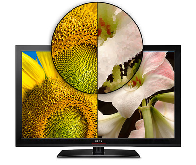
Fourfold increase in TV screen resolution
A new video standard enables a fourfold increase in the resolution of TV screens, and an MIT chip was the first to handle it in real time.
It took only a few years for high-definition televisions to make the transition from high-priced novelty to ubiquitous commodity - and they now seem to be heading for obsolescence just as quickly. Now manufacturers are debuting new ultrahigh-definition, or UHD, models (also known as 4K or Quad HD) with four times the resolution of today’s HD TVs.
In addition to screens with four times the pixels, however, UHD also requires a new video-coding standard, known as high-efficiency video coding, or HEVC. Broadcom has already announced the first commercial HEVC chip, which it said will go into volume production in mid-2014.
MIT researchers have also unveiled a HEVC chip. The researchers’ design was executed by the Taiwan Semiconductor Manufacturing Company, through its University Shuttle Program, and Texas Instruments (TI) funded the chip’s development.

Although the MIT chip isn’t intended for commercial release, its developers believe that the challenge of implementing HEVC algorithms in silicon helps illustrate design principles that could be broadly useful. Moreover, “because now we have the chip with us, it is now possible for us to figure out ways in which different types of video data actually interact with hardware,” says Mehul Tikekar, an MIT graduate student in electrical engineering and computer. “People don’t really know, ‘What is the hardware complexity of doing, say, different types of video streams?’”
In the pipeline
Like older coding standards, the HEVC standard exploits the fact that in successive frames of video, most of the pixels stay the same. Rather than transmitting entire frames, it’s usually enough for broadcasters to transmit just the moving pixels, saving a great deal of bandwidth. The first step in the encoding process is thus to calculate ‘motion vectors’ - mathematical descriptions of the motion of objects in the frame.
On the receiving, end, however, that description will not yield a perfectly faithful image, as the orientation of a moving object and the way it’s illuminated can change as it moves. So the next step is to add a little extra information to correct motion estimates that are based solely on the vectors. Finally, to save even more bandwidth, the motion vectors and the corrective information are run through a standard data-compression algorithm, and the results are sent to the receiver.
The new chip performs this process in reverse. It was designed by researchers in the lab of Anantha Chandrakasan, the Joseph F and Nancy P Keithley Professor of Electrical Engineering and head of the MIT Department of Electrical Engineering and Computer Science. In addition to Chandrakasan and Tikekar, these include Chiraag Juvekar, another graduate student in Chandrakasan’s group; former postdoc Chao-Tsung Huang; and former graduate student Vivienne Sze, now at TI.
The chip’s first trick for increasing efficiency is to ‘pipeline’ the decoding process: A chunk of data is decompressed and passed to a motion-compensation circuit, but as soon as the motion compensation begins, the decompression circuit takes in the next chunk of data. After motion compensation is complete, the data passes to a circuit that applies the corrective data and, finally, to a filtering circuit that smooths out whatever rough edges remain.
Finetuning
Pipelining is fairly standard in most video chips, but the MIT researchers developed a couple of other tricks to further improve efficiency. The application of the corrective data, for instance, is a single calculation known as matrix multiplication. A matrix is just a big grid of numbers; in matrix multiplication, numbers in the rows of one matrix are multiplied by numbers in the columns of another, and the results are added together to produce entries in a new matrix.
“We observed that the matrix has some patterns in it,” Tikekar explains. In the new standard, a 32-by-32 matrix, representing a 32-by-32 block of pixels, is multiplied by another 32-by-32 matrix, containing corrective information. In principle, the corrective matrix could contain 1024 different values. But the MIT researchers observed that, in practice, “there are only 32 unique numbers”, Tikekar says. “So we can efficiently implement one of these [multiplications] and then use the same hardware to do the rest.”
Similarly, Juvekar developed a more efficient way to store video data in memory. The “naive way”, he explains, would be to store the values of each row of pixels at successive memory addresses. In that scheme, the values of pixels that are next to each other in a row would also be adjacent in memory, but the value of the pixels below them would be far away.
In video decoding, however, “it is highly likely that if you need the pixel on top, you also need the pixel right below it”, Juvekar says. “So we optimise the data into small square blocks that are stored together. When you access something from memory, you not only get the pixels on the right and left, but you also get the pixels on the top and bottom in the same request.”
Chandrakasan’s group specialises in low-power devices, and in ongoing work, the researchers are trying to reduce the power consumption of the chip even further, to prolong the battery life of quad-HD mobile phones or tablet computers. One design modification they plan to investigate, Tikekar says, is the use of several smaller decoding pipelines that work in parallel. Reducing the computational demands on each group of circuits would also reduce the chip’s operating voltage.
3D-printed, shape-shifting antenna inspired by sci-fi
Researchers at the Johns Hopkins Applied Physics Laboratory in Laurel, Maryland, have created an...
Researchers knit 'blanket' of radio-frequency antennas
Researchers have used traditional flat-knitting techniques to fabricate flexible and lightweight...
Unlocking next-gen chip efficiency
By studying how heat moves through ultra-thin metal layers, researchers have provided a...


