Energy-efficient switches would enable next-gen data centres

With demand for data growing exponentially, there is increasing pressure for data centres to become more energy efficient. A team led by University of Washington (UW) scientists has now reported the design of a silicon-based non-volatile switch that would greatly reduce the energy needs of data centres, with their results published in the journal Nature Nanotechnology.
One way to reduce energy consumption in data centres is to use light to communicate information, with electrically controlled optical switches controlling the flow of light — and therefore information — between servers. These optical switches need to be multifunctional and energy efficient to support the continued expansion of data centres.
Silicon photonic switches are widely used in part because they can be made using well-established semiconductor fabrication techniques. Traditionally, these switches have been tuned through thermal effect — a process where heat is applied, often by passing a current through a metal or semiconductor, to change the optical properties of a material in the switch, thus changing the path of the light. However, not only is this process not energy efficient, but the changes it induces are not permanent. As soon as the current is removed, the material reverts to its previous state and the connection — and flow of information — is broken.
To address this, researchers from UW, Stanford University, Charles Stark Draper Laboratory, the University of Maryland and the Massachusetts Institute of Technology (MIT) created a ‘set and forget’ switch capable of maintaining the connection without any additional energy. They used a phase-change material that is non-volatile, meaning the material is transformed by briefly heating it, and it remains in that state until it receives another heat pulse, at which point it reverts back to its original state. This eliminates the need to constantly input energy to maintain the desired state.
Previously, researchers have used doped silicon to heat the phase-change material. Silicon alone doesn’t conduct electricity, but when selectively doped with different elements like phosphorus or boron, silicon is able to both conduct electricity and propagate light without any excess absorption. When a current is pumped through the doped silicon, it can act like a heater to switch the state of the phase-change material on top of it. The catch is that this is also not a very energy-efficient process — the amount of energy needed to switch the phase-change material is similar to the amount of energy used by traditional thermo-optic switches. This is because the entire 220 nm-thick doped silicon layer has to be heated to transform only 10 nm of phase-change material. A lot of energy is wasted heating such a large volume of silicon to switch a much smaller volume of phase-change material.
“We realised we had to figure out how to reduce the volume that needed to be heated in order to boost the efficiency of the switches,” said lead and co-corresponding author Zhuoran (Roger) Fang, a PhD student at UW.
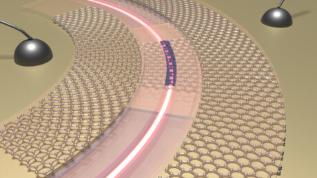
One approach would be to make a thinner silicon film, but silicon doesn’t propagate light well if it is thinner than 200 nm. So instead, they used an un-doped 220 nm silicon layer to propagate light and introduced a layer of graphene between the silicon and phase-change material to conduct electricity. Like metal, graphene is an excellent conductor of electricity, but unlike metal, it is atomically thin — it consists of just a single layer of carbon atoms arranged in a two-dimensional honeycomb lattice. This design eliminates wasted energy by directing all heat generated by the graphene to go towards changing the phase-change material. In fact, the switching energy density of this set-up is only 8.7 attojoules (aJ)/nm3, a 70-fold reduction compared to doped silicon heaters, the current state of the art. This is also within one order of magnitude of the fundamental limit of switching energy density (1.2 aJ/nm3).
Even though using graphene to conduct electricity induces some optical losses, meaning some light is absorbed, graphene is so thin that not only are the losses minimal, but the phase-change material can still interact with the light propagating in the silicon layer. The team established that a graphene-based heater can reliably switch the state of the phase-change material more than 1000 cycles. This is a notable improvement over the doped silicon heaters, which have only been shown to have an endurance of around 500 cycles.
“Even 1000 is not enough,” said corresponding author Arka Majumdar, an associate professor at UW. “Practically speaking, we need about a billion cycles endurance, which we are currently working on.”
Now that they have demonstrated that light can be controlled using a phase-change material and graphene heater, the team plans to show that these switches can be used for optical routing of information through a network of devices, a key step towards establishing their use in data centres. They are also interested in applying this technology to silicon nitride for routing single photons for quantum computing.
“The ability to be able to tune the optical properties of a material with just an atomically thin heater is a game changer,” Majumdar said. “The exceptional performance of our system in terms of energy efficiency and reliability is really unheard of and could help advance both information technology and quantum computing.
“Compared with what is currently being used in data centres to control photonic circuits, this technology would greatly reduce the energy needs of data centres, making them more sustainable and environmentally friendly.”
Please follow us and share on Twitter and Facebook. You can also subscribe for FREE to our weekly newsletter and bimonthly magazine.
Spinning, twisted light could power next-generation electronics
Researchers have created an organic semiconductor that forces electrons to move in a spiral...
Improving the way flash memory is made
Researchers are developing the ideal manufacturing process for a type of digital memory known as...
Optical memory unit boosts processing speed
Researchers have developed a fast, versatile volatile photonic memory that could enhance AI,...


