
2D electronics take a step forward
Scientists at Rice University and Oak Ridge National Laboratory (ORNL) have advanced on the goal of two-dimensional electronics with a method to control the growth of uniform atomic layers of molybdenum disulfide (MDS).
MDS, a semiconductor, is one of a trilogy of materials needed to make functioning 2D electronic components. The Rice labs of lead investigator Jun Lou, Pulickel Ajayan and Boris Yakobson, all professors in the university’s Mechanical Engineering and Materials Science Department, collaborated with Wigner Fellow Wu Zhou and staff scientist Juan-Carlos Idrobo at ORNL in an unusual initiative that incorporated experimental and theoretical work.
Their goals were to see if large, high-quality, atomically thin MDS sheets could be grown in a chemical vapour deposition (CVD) furnace and to analyse their characteristics. The hope is that MDS could be joined with graphene, which has no band gap, and hexagonal boron nitride (hBN), an insulator, to form field-effect transistors, integrated logic circuits, photo detectors and flexible optoelectronics.
The study of graphene prompted research into a lot of 2D materials; molybdenum disulfide is just one of them, said Ajayan.
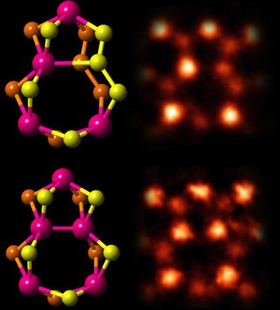
MDS is distinct from graphene and hBN because it isn’t exactly flat. Graphene and hBN are flat, with arrays of hexagons formed by their constituent atoms. But while MDS looks hexagonal when viewed from above, it is actually a stack, with a layer of molybdenum atoms between two layers of sulfur atoms.
Co-author Zheng Liu, a joint research scientist in Lou’s and Ajayan’s labs, noted the Yakobson group predicted that MDS and carbon atoms would bind. “The question now is how to bring all the 2D materials together,” said co-author Sina Najmaei, a Rice graduate student.
Until recently, growing MDS in a usable form has been difficult. The ‘Scotch tape’ method of pulling layers from a bulk sample has been tried, but the resulting materials were inconsistent, Lou said. Early CVD experiments produced MDS with grains that were too tiny to be of use for their electrical properties.
But in the process, the researchers noticed ‘islands’ of MDS tended to form in the furnace where defects or even pieces of dust appeared on the substrate. “The material is difficult to nucleate, unlike hBN or graphene,” Najmaei said. “We started learning that we could control that nucleation by adding artificial edges to the substrate, and now it’s growing a lot better between these structures.”
“Now we can grow grain sizes as large as 100 microns,” Lou said. That’s still only about the width of a human hair, but in the nanoscale realm, it is big enough to work with, he said.
Once the Ajayan and Lou teams were able to grow such large MDS arrays, the ORNL team imaged the atomic structures using aberration-corrected scanning transmission electron microscopy. The atomic array can clearly be seen in the images and, more importantly, so can the defects that alter the material’s electronic properties.
With ORNL’s images in hand, theoretical physicist Yokobson and his team were not only able to calculate the energies of a much more complex set of defects than are found in graphene or BN but could also match their numbers to the images.
The Rice researchers see many possible ways to combine the materials, not only in two-dimensional layers but also as three-dimensional stacks. “Now we have the opportunity to build 3D crystals with different compositions,” Lou said.
“These are very different materials, with different electronic properties and band gaps. Putting one on top of the other would give us a new type of material that we call van der Waals solids,” Ajayan said. “We could put them together in whatever stacking order we need, which would be an interesting new approach in materials science.
Co-authors of the Nature Materials paper are Rice research associate Xiaolong Zou, graduate students Gang Shi and Sidong Lei, and Wu Zhou at Oak Ridge National Laboratory. The Welch Foundation, the National Science Foundation (NSF), the US Army Research Office, the US Office of Naval Research, the Nanoelectronics Research Corporation and the Department of Energy supported the work.
Spinning, twisted light could power next-generation electronics
Researchers have created an organic semiconductor that forces electrons to move in a spiral...
Improving the way flash memory is made
Researchers are developing the ideal manufacturing process for a type of digital memory known as...
Optical memory unit boosts processing speed
Researchers have developed a fast, versatile volatile photonic memory that could enhance AI,...


")