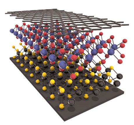
New technique to measure 2D wonder materials

A research team led by the University of Warwick has developed a method to measure the electronic structures of stacks of two-dimensional materials, whose features such as flatness, atomic thinness, high conductivity and extreme strength make them highly desirable for use in electronic devices.
Multiple stacked layers of 2D materials — known as heterostructures — create highly efficient optoelectronic devices with ultrafast electrical charge, which can be used in nanocircuits and are stronger than materials used in traditional circuits. Various heterostructures have been created using different 2D materials, while stacking different combinations of 2D materials creates new materials with new properties.
The new technique, created by Dr Neil Wilson, measures the electronic properties of each layer in a stack, allowing researchers to establish the optimal structure for the fastest, most efficient transfer of electrical energy. It uses the photoelectric effect to directly measure the momentum of electrons within each layer and shows how this changes when the layers are combined.
The ability to understand and quantify how 2D material heterostructures work — and to create optimal semiconductor structures — paves the way for the development of highly efficient nanocircuitry and smaller, flexible, more wearable gadgets. Solar power could also be revolutionised with heterostructures, as the atomically thin layers allow for strong absorption and efficient power conversion with a minimal amount of photovoltaic material.
“It is extremely exciting to be able to see, for the first time, how interactions between atomically thin layers change their electronic structure,” said Dr Wilson.
The technique has been published in the journal Science Advances.
Electronex Sydney a major success
More than 1000 trade visitors and delegates have attended the Electronics Design & Assembly...
Gartner: Global AI chips revenue to grow 33% in 2024
Gartner has forecast that the revenue from AI semiconductors globally will total $71 billion in...
Electronex Expo returns to Sydney for 2024
Electronex — the Electronics Design and Assembly Expo will return to Sydney in 2024,...


