Sinterless route to 3D printing nanoscale optical-grade glass

Printing of micro- and nanometre-scaled quartz glass structures from pure silicon dioxide opens up many new applications in optics, photonics and semiconductor technologies. So far, processes have been based on conventional sintering. Temperatures required for sintering silicon dioxide nanoparticles are above 1100°C, which is much too hot for direct deposition onto semiconducting chips. A team headed by Dr Jens Bauer from KIT’s Institute of Nanotechnology (INT) has now developed a new process to produce transparent quartz glass with a high resolution and excellent mechanical properties at far lower temperatures.
The Karlsruhe Institute of Technology (KIT) has developed a new process that enables printing of nanometre-scale quartz glass structures directly onto semiconductor chips. A hybrid organic-inorganic polymer resin is used as feedstock material for 3D printing of silicon dioxide. Since the process works without sintering, the required temperatures are lower, while the increased resolution enables visible-light nanophotonics. The research findings have been published in Science.
The printing of micro- and nanometre-scaled quartz glass structures from pure silicon dioxide opens up new applications in optics, photonics and semiconductor technologies. So far, processes have been based on conventional sintering. Temperatures required for sintering silicon dioxide nanoparticles are above 1100°C, which is too hot for direct deposition onto semiconducting chips. A team led by Dr Jens Bauer from KIT has developed a new process to produce transparent quartz glass with a high resolution and excellent mechanical properties at lower temperatures.
Bauer and his colleagues from the University of California, Irvine and the Edwards Lifesciences Company in Irvine presented the process in Science. The researchers used a hybrid organic-inorganic polymer resin as the feedstock material. This liquid resin consists of so-called polyhedral oligomeric silsesquioxane (POSS) molecules, which are small cage-like silicon dioxide molecules equipped with organic functional groups.
After cross-linking the material via 3D printing to form a 3D nanostructure, it is heated to 650°C in air to remove the organic components. At the same time, the inorganic POSS cages coalesce and form a continuous quartz glass microstructure or nanostructure. The temperature required for this purpose is only half the temperature needed for processes based on sintering of nanoparticles.
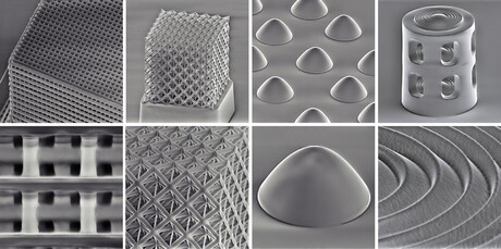
Bauer said that the lower temperature enables the free-form printing of robust, optical-grade glass structures with the resolution needed for visible-light nanophotonics, directly on semiconductor chips. Apart from the high optical quality, the quartz glass produced also has excellent mechanical properties and can be processed easily. The researchers used the POSS resin to print various nanostructures, including photonic crystals of free-standing, 97 nm wide beams, parabolic microlenses and a multi-lens micro objective with nanostructured elements. “Our process produces structures that remain stable even under harsh chemical or thermal conditions,” Bauer said.
Professor Oliver Kraft, Vice President Research of KIT, said the research group headed by Jens Bauer is associated with the 3DMM2O Cluster of Excellence. “The research results now published in Science are only one example of how early-stage researchers are successfully supported in the cluster,” Kraft said.
3D Matter Made to Order, or 3DMM2O, is a joint Cluster of Excellence by KIT and Heidelberg University. It is aimed at raising 3D additive manufacture to the next level — from the level of molecules up to macroscopic dimensions.
Terahertz wave control for enhanced wireless technology
Researchers have developed a new patterned spintronic emitter that enables room-temperature...
Upcycling battery waste and CO2 into fuel
Researchers from TU Wien have produced a nanocatalyst based on spent batteries and aluminium foil...
Evaluating the commercial viability of sustainable perovskite LEDs
Researchers have discovered that perovskite LEDs have great long-term commercial potential,...


