Impacts of 3D stacking photonic and electronic chips

Recent advancements in AI and in large language models such as ChatGPT have put a strain on data centres, as AI models require large amounts of data to train — in order to move data between the processing units and memory, efficient communication links become necessary. Fibre optics have been the go-to solution for long distance communication, with the industry starting to adopt them for short distance intra-data centre communication too. Recent technological developments have enabled the switch from electrical to optical interconnect for small distances, such as the communication between chips inside the same package.
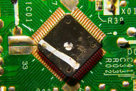
This requires a conversion of the data stream from the electrical to the optical domain, which happens in the optical transceiver. Silicon photonics are widely used to fabricate these optical transceivers. The active photonic devices inside the chip — modulators and photodetectors — still require a connection with electronic drivers for powering the devices and reading the incoming data. Stacking the electronic chip (EIC) on top of the photonic chip (PIC) through 3D sticking technology realises a tight integration of the components with low parasitic capacitance.
In research published in the Journal of Optical Microsystems, researchers from KU Leuven and imec in Belgium investigated the thermal impact of this 3D integration. The design of the photonic chip consists of an array of ring modulators, which are known for their temperature sensitivity. In order to operate in a demanding environment, such as a data centre, they need active thermal stabilisation. This is implemented as an integrated heater.
The researchers measured the heater efficiency of the ring modulators before and after flip-chip bonding of the EIC on the PIC. A relative loss of 43.3% in efficiency was found. Furthermore, 3D finite element simulations attributed this loss to heat spreading in the EIC. This should be avoided, because in the ideal case all heat that is generated in the integrated heater is contained close to the photonic device. The thermal crosstalk between the photonic devices also increased by up to +44.4% after bonding the EIC, which complicates the individual thermal control.
To prevent heater efficiency loss, the researchers also conducted a thermal simulation study where typical design variables were changed. The research findings showed that by increasing the spacing between µbumps and the photonic device, and by decreasing the interconnect linewidth, the thermal penalty of 3D integration can be minimised.
Terahertz wave control for enhanced wireless technology
Researchers have developed a new patterned spintronic emitter that enables room-temperature...
Upcycling battery waste and CO2 into fuel
Researchers from TU Wien have produced a nanocatalyst based on spent batteries and aluminium foil...
Evaluating the commercial viability of sustainable perovskite LEDs
Researchers have discovered that perovskite LEDs have great long-term commercial potential,...


