Atom by atom: building a silicon quantum computer chip

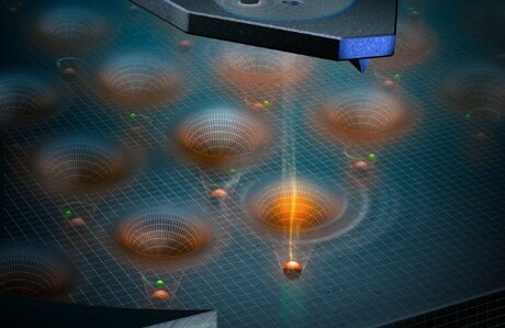
Australian and German researchers have developed a technique for embedding single atoms in a silicon wafer one by one, offering the potential to make quantum computers using the same methods that have given us cheap and reliable conventional devices containing billions of transistors.
The new technique, described in the journal Advanced Materials, can create large-scale patterns of counted atoms that are controlled so their quantum states can be manipulated, coupled and read out. Lead author Professor David Jamieson, from The University of Melbourne, said the team’s vision was to use this technique to build a very, very large-scale quantum device.
“We believe we ultimately could make large-scale machines based on single-atom quantum bits by using our method and taking advantage of the manufacturing techniques that the semiconductor industry has perfected,” Prof Jamieson said.
Until now, implanting atoms in silicon has been a haphazard process, where a silicon chip gets showered with phosphorus which implants in a random pattern. Study co-author Scientia Professor Andrea Morello, from UNSW Sydney, said the new technique embeds phosphorus ions, precisely counting each one, in a silicon substrate creating a qubit ‘chip’, which can then be used in lab experiments to test designs for large-scale devices.
“This will allow us to engineer the quantum logic operations between large arrays of individual atoms, retaining highly accurate operations across the whole processor,” Prof Morello said.
“Instead of implanting many atoms in random locations and selecting the ones that work best, they will now be placed in an orderly array, similar to the transistors in conventional semiconductor computer chips.”
The technique takes advantage of the precision of the atomic force microscope, which has a sharp cantilever that responds to the force fields above the surface of a chip with a positioning accuracy of just half a nanometre, about the same as the spacing between atoms in a silicon crystal. The team drilled a tiny hole in this cantilever, so that when it was showered with phosphorus atoms one would occasionally drop through the hole and embed in the silicon substrate.
The key was knowing precisely when a single atom had become embedded in the substrate, at which point the cantilever could move to the next precise position on the array. The team discovered that the kinetic energy of the atom as it ploughs into the silicon crystal and dissipates its energy by friction can be exploited to make a tiny electronic ‘click’, which the team could ‘hear’ as each atom dropped into one of the 10,000 sites in the prototype device.
“One atom colliding with a piece of silicon makes a very faint click, but we have invented very sensitive electronics used to detect the click; it’s much amplified and gives a loud signal,” Prof Jamieson said.
“That allows us to be very confident of our method.”
First author Dr Alexander (Melvin) Jakob, from The University of Melbourne, said the collaborators utilised advanced technology developed for sensitive X-ray detectors and a special atomic force microscope originally developed for the Rosetta space mission, along with a comprehensive computer model for the trajectory of ions implanted into silicon.
“We have already produced groundbreaking results on single-atom qubits made with this technique, but the new discovery will accelerate our work on large-scale devices,” he said.
Please follow us and share on Twitter and Facebook. You can also subscribe for FREE to our weekly newsletter and bimonthly magazine.
Terahertz wave control for enhanced wireless technology
Researchers have developed a new patterned spintronic emitter that enables room-temperature...
Upcycling battery waste and CO2 into fuel
Researchers from TU Wien have produced a nanocatalyst based on spent batteries and aluminium foil...
Evaluating the commercial viability of sustainable perovskite LEDs
Researchers have discovered that perovskite LEDs have great long-term commercial potential,...


