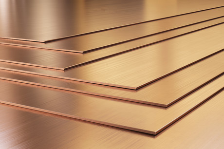
Solid copper base hybrid PCBs

Heat generation in electronic circuits creates a level of inefficiency; however, it is almost impossible to create a circuit that operates at 100% efficiency as the laws of physics and thermodynamics demonstrate this through the fundamentals of temperature, energy and entropy. Therefore, we must accept that any electronic circuit will generate some amount of heat when it is in operation and account for this in the initial design process.
As most electronic components are now available as miniature and surface mount technology, removal of heat from these devices can create an issue, especially when mounting them on a printed circuit board (PCB) — one that may be a poor conductor of heat.
A typical PCB has an insulating core, which also does not conduct heat very well. Although there are copper traces present, the amount of heat conducted by conventional PCBs depends on their design specifically regarding the surface area of the copper traces. It is known that broad traces will conduct heat more efficiently than thin traces. Engineers eliminate the problem of heat conduction, drawing heat away from the PCB by using metal core PCBs (MCPCBs). The MCPCBs utilise a metal core as the base material, replacing FR4 or CEM3 which are most commonly utilised.
Why use copper?
As copper has high thermal conductivity, it is an efficient choice for use as a heat sink in MCPCBs. Circuit traces, necessary to interconnect various components on the PCB, remain electrically insulated from the base metal core as there is a thermally conductive dielectric layer separating them. This dielectric layer bonds the circuit traces to the base metal. The thermal performance of any MCPCB depends exclusively on this dielectric layer.
MCPCBs with solid copper bases are utilised by engineers for mounting LED lights, due to the high thermal conductivity and efficiency. Although an SMD LED is a high-efficiency device and converts a major part of its input power into visible light, a minor part generates waste heat within the LED chip. Therefore, high-power LED lights will tend to generate more heat as a wasted by-product. Unless this by-product is removed, this waste heat build-up can be fatal to the function of the LED.
Creating efficiency
Engineers design the removal of the excess heat from the LEDs on the PCB in two main ways: by using broad traces of copper to interconnect the LEDs with the rest of the circuit and/or by adding a solid copper base creating insulation with a thermally conducting dielectric. For medium-power LEDs, the terminals conduct the heat generated from within the LED chip to the broad traces to which the terminals are soldered, dissipating the heat effectively. Part of the heat also travels through the thermally conducting dielectric to the solid copper base, which serves as the ultimate heat sink.
For high-power LEDs and circuits generating copious amounts of heat, additional channels are necessary to conduct more of the heat into the solid copper base. Engineers handle this with two additional mechanisms: through a heat-conducting metal tab under the LED or through the IC attached to its internal die while implementing the use of metal-filled thermal vias.
By incorporating a copper land immediately under the device, the IC or LED can transfer the heat from its die through the metal tab directly to the copper land. Therefore, multiple metal-filled thermal vias, connecting the copper land to the solid copper base effectively, can transfer enough heat to the heat sink to keep the LED or IC cool and operating safely.
Case study: Aluminium vs copper
We know that the lighting industry in particular has driven aluminium PCB fabrication technologies to date in various thicknesses in a one-, two- and four-layer construction, but the less complex, more specialised hybrid aluminium PCB has also seen an increase in production as a simpler version of construction and a more complex circuit design in a two-layer version.
Traditionally, electronics engineers would design a standard 1.6 mm two-layer PCB which would then be bonded to 1.5 mm of aluminium via a 0.3 mm thermal conductive prepreg layer, all of which works well — except that transferring heat through a 1.6 mm FR4 material + 0.3 mm prepreg is inefficient. So electronics engineers started design hybrid PCBs with thinner and thinner two-layer FR4 cores, which makes sense to increase the heat-transferring efficiency by decreasing the distance between copper tracks and aluminium substrate — but this has its limitations.
A project that was recently fabricated by PCB Global required a hybrid PCB, with the original design created as a 3 mm aluminium-based hybrid PCB with a 0.2 mm thermal conductive dielectric prepreg layer and 0.3 mm two-layer PCB. We experienced an unexpected outcome after pressing the 0.3 mm FR4 to the 3 mm aluminium substrate. The top-layer FR4 circuit became distorted and the solder paste stencil did not align. This was a great mystery, as the design file provided did not seem to have any flaws.
Investigation
With further detailed investigations, we concluded that the tensile strength of the aluminium base material was too high at approximately 310 MPa. When pressing the 0.3 mm FR4 under standard multilayer heat and pressure fabrication conditions, the thin substrate 0.3 mm FR4 (even with a high TG=170 material) tended to reach its glass transition temperature (TG), creating movement and distortion around 0.17 mm across a 375 mm long PCB.
Solution
The 3 mm aluminium metal base was substituted for a 3 mm solid copper base material. Copper has a much lower tensile strength of 200 MPa and we soon discovered that the issue of distortion was completely eliminated, thus resulting in a more efficient heat-dissipating product and also increasing the longevity of the product.

FR4 core — 0.3 mm
Copper — 18 µm plated 35 µm
Pre-preg 7628HR 0.2 mm
Our company
At PCB Global, we continuously encounter many challenges experienced by our customers in their design process and we have always progressed towards finding a solution that is both efficient and beneficial to customers’ requirements. Quotes and orders are processed 24 hours a day, seven days a week and 365 days a year on our easy-to-follow online portal, to which automated instant quotes are created by you to your specifications. Please don’t hesitate to contact us at sales@pcbglobal.com or, to find out more about our company, please visit www.pcbglobal.com.
Brain-inspired AI hardware advances neuromorphic systems
Autonomous devices can operate more smartly and efficiently thanks to neuromorphic hardware that...
Brain-inspired chip material cuts AI energy demands
A novel chip material inspired by the human brain could lower AI energy use by mimicking neural...
Superconductor advance targets low-power electronics design
Researchers have developed a superconducting material for electronics, reducing energy loss and...


