The secret of big digital chip design is all in the NoC
Tuesday, 06 October, 2020

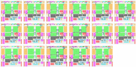
Sondrel is known for designing very large digital chips, and the secret lies in its ability to ensure that data flows around the chip between blocks correctly using a network on chip (NoC). Without an NoC, a chip could need up to 10 times more memory to operate in a similar manner without latency, which would be uneconomical.
In an ideal design, all the sections that need high-speed, high data flow between them would be located as close together as possible, ie, memory in the middle of the chip next to the blocks of IP (intellectual property) that need memory access. In reality, apart from cache, memory is located off-chip on dedicated memory chips, which use state-of-the-art memory technologies, so that access points to memory are located on the perimeter of the chip. As a result, a complex network of interconnections is needed to route the data traffic between blocks and to and from off-chip memory. On a big chip design, there could be 17 layers of horizontal interconnections plus a number of vertical connections between these layers.
“It’s rather like designing a massive, multilevel office block where you have to design it to allow for optimal movement of people between areas and floors,” explained Anne-Françoise Brenton, Sondrel’s NoC expert.
“Where a lot of people need to move rapidly between two locations, you need a wide, fast corridor and the length of it affects the timing of the arrival of people. Similarly, an infrequently used, non-urgent route can be long and narrow, and therefore slow.
“The analogy continues with the vertical interconnects being lifts with big capacity, lifts that just connect two specific floors to provide a dedicated route for high-speed connections, and lifts that stop at all floors that are slower but connect a lot of locations. On top of this is the arbitration that dynamically controls the data flow through the NoC with buffering to smooth and optimise as demand changes, for example when two IP blocks are sharing and accessing the same memory.”
Designing the NoC is an iterative collaboration throughout the entire chip design process between the front end, the back end and NoC teams of designers, as any changes can have a knock-on effect to the other’s work. As the front-end design of the chip layout crystallises, the requirement of the NoC to arbitrate the load demands becomes clearer — which it does by keeping track of the data and its location in cache, off-chip memory or being processed in an IP block.
One of the challenges in NoC design is that third-party IP blocks can be a black box solution with very little data provided on its demands for data flow, as the vendor wants to protect the exact workings of its IP. This is overcome as the whole design matures by using timing analysis to help ensure that the NoC is delivering the data as required by arbitrating the pathways to deliver the data according to pre-assigned priorities — there cannot be any bottlenecks.
“NoC design is a constantly changing juggling act,” Brenton concluded. “Change one parameter and several other things could change. It’s as intellectually challenging as playing several games of chess simultaneously and it is immensely rewarding.”
Please follow us and share on Twitter and Facebook. You can also subscribe for FREE to our weekly newsletter and bimonthly magazine.
Turning peanut waste into graphene for next-gen electronics
UNSW Sydney engineers have developed a cheaper and greener way to make graphene from leftover...
Light-powered optical modules boost AI efficiency
Researchers have developed a new generation of AI hardware that runs on light instead of...
New materials could boost the energy efficiency of microelectronics
By stacking multiple active components based on new materials on the back end of a computer chip,...


